
This report analyzes the random telegraph signal (RTS) waveform response of YBCO nanowire detectors under varying bias currents, using both experimental observation and circuit simulation. The study reveals a bias-dependent resistance switching behavior and discusses its implications for photoresponse dynamics and device latching effects.
The RTS waveform evolution
Testing Methods and Observation
To facilitate your understanding and analysis of our device response characteristics, let me first introduce the electrical connections of our testing system. Our YBCO devices are fabricated on a 5mm × 5mm STO substrate. They are encapsulated in a sample holder using wire bonding (as shown in Figure 1a) and connected to SMA cables (as shown in Figure 1b). The bias tee and low-noise amplifier (LNA 70dB) are connected in the first cold stage area (as shown in Figure 1c). The DC bias for the bias tee is provided by Keithley 2400 source meter, and the amplifier output is connected to an oscilloscope.
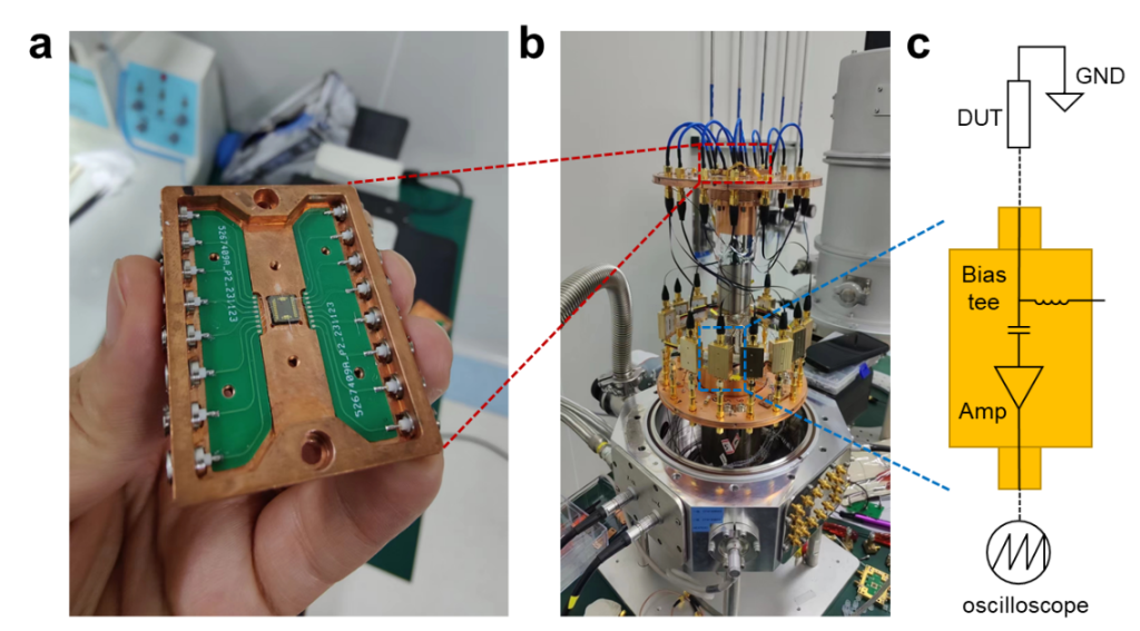 Figure 1 Testing system and readout circuit, a detector chip encapsulated into a sample holder, b test refrigeration unit, sample placed on the second-stage cold platform and connected to the bias tree and amplifier of the first-stage cold platform via SMA cables, c schematic diagram of the readout circuit.
As demonstrated in the previous email, based on the above testing system, our YBCO nanowire devices exhibit different response waveforms at different bias currents. These waveforms all appear near the Is. The device current scan IV curves (Figure 2a-b) and oscilloscope video screenshots (Figure 2c-f) at different bias current as shown below. You can find the complete video in the email attachment.
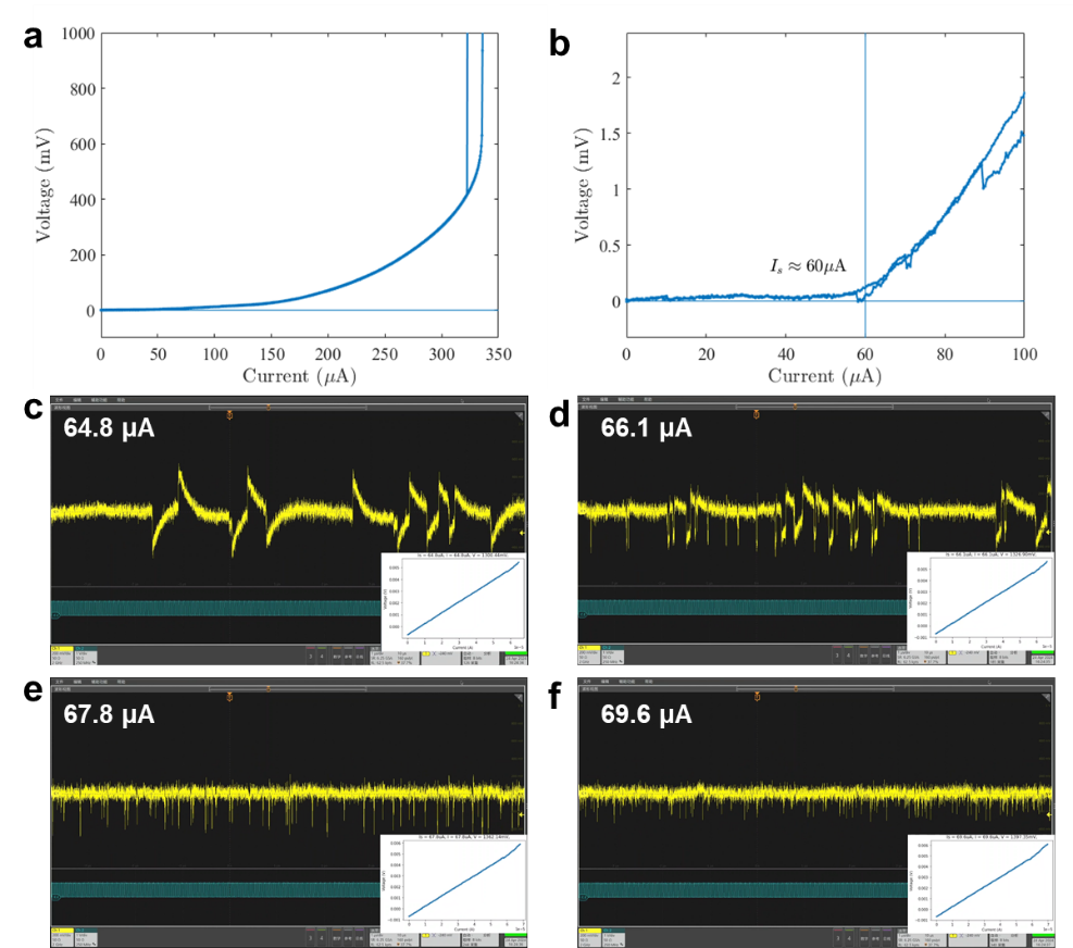 Figure 2 Electrical steady-state scan and transient response of the device, a-b device current scan IV curves, c-f transient response waveforms under different current biases.
Circuit Model and Waveform Interpretation
Firstly, regarding the upwarp in the IV curve, we believe it is due to dissipation introduced by vortex flux flow across the nanowire, which leads to a finite voltage in the direction of the nanowires when bias current larger than Is, as reported in Dobrovolskiy ‘s study (Phys. Rev. B 105, 214507, 2022). In contrast, based on the resistance caused by flux flow dissipation, our device exhibits a slight resistance jump near Is under biasing. This jump in voltage is significantly smaller than the dissipation voltage generated by vortex flux flow. This voltage jump is amplified by the amplifier and then captured by the oscilloscope. Based on this phenomenon, we simplify it as a resistance random switch between Rflux and Rflux+Rv. Here, Rflux represents the macroscopic resistance caused by vortex flux flow, while Rv represents the slight switch resistance. We configured the circuit model and simulated the transient response based on Simulink. The schematic diagram of the circuit is as Figure 3.
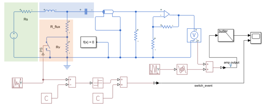 Figure 3 Circuit simulation schematic based on Simscape in Simulink, where the orange area represents simplified devices, the blue area represents the bias tree, and the green area represents the external current bias source.
Through the simulation, we can explain that the evolution of this waveform is due to the increase in the frequency of device resistance random switching with the increase in bias current. This random process is often referred as random telegraph signals (RTS), which are often interpreted as “Grain boundary junctions” (Appl. Phys. Lett. 78, 955–957, 2001) or “Two Level Fluctuate” (https://research.chalmers.se/en/publication/515677 chapter 6.5). And it’s worth noting that the decay of pulses is not caused by dynamic inductance but rather by the charging and discharging of capacitors in the bias tree. Since the detector’s kinetic inductance is small, the decay of pulse response should be on the order of 100 picoseconds. This explains why short pulses can be observed under relatively high bias currents (as shown in Figure 4c-d).
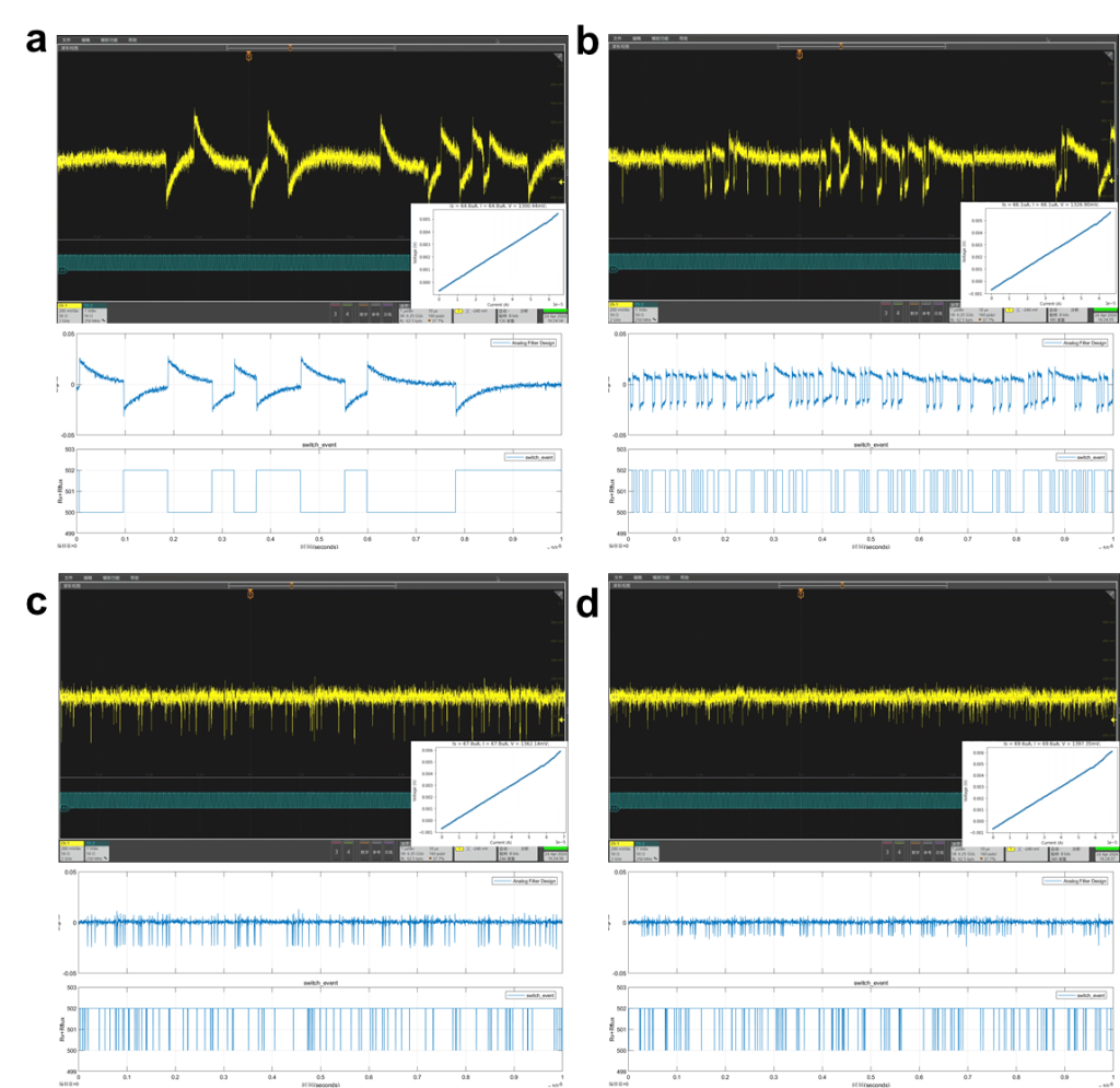 Figure 4 Comparison between measured waveform and simulation results
Pulsed light response and latching
In our experiment, when we used pulsed light to irradiate the core region of the device, we observed that the falling edge of the device response waveform synchronized with the pulse light event under relatively low bias, but the rising edge was unrelated to the pulse light event. Based on the above analysis, this implies that when the device is in the Rflux+Rv state, it will be triggered by a photon pulse and switch to the Rflux state. However, the Rflux state is inert to photon pulses, and it can only wait for the device to spontaneously switch back to the Rflux+Rv state. This process is akin to the device being latched into the Rflux state. At relatively large bias currents, although the device’s switching frequency is high and it does not remain latched for long time. But our low quantum efficiency results in optical counts far below the device’s spontaneous switching (or dark counts), making it indistinguishable.
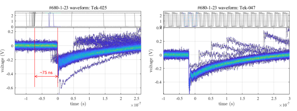 Figure 5 Oscilloscope fluorescence waveform diagram (superposition of 100 waveforms), device pulse edge and pulse light event are synchronized
This type of latching seems different from traditional SNSPDs and is not caused by localized hotspots maintaining. We have tried some strategies to address this issue, such as fabricating longer meandering lines or parallel inductor-resistor shunt circuit, but they have not yielded significant improvements. We would like to ask if you have any other ideas for addressing this phenomenon.
Simulation file: RTSwaveform.slx
Figure file: RTS-waveform-figure.pptx